Company Overview
PHILIPS TECHNICAL SERVICES EXPERTS IN HDI PCB DESIGN.
PTS has been in business since 2013. With over 40 years of experience designing HDI printed circuit boards Military and Commercial application. We are experts in expediting workload and cutting costs and freeing up employees many companies keeping them on schedule sometimes do to in house procedures.
CORE COMPETENCIES:
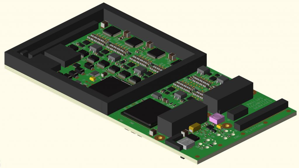
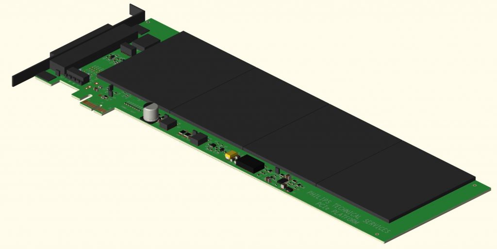
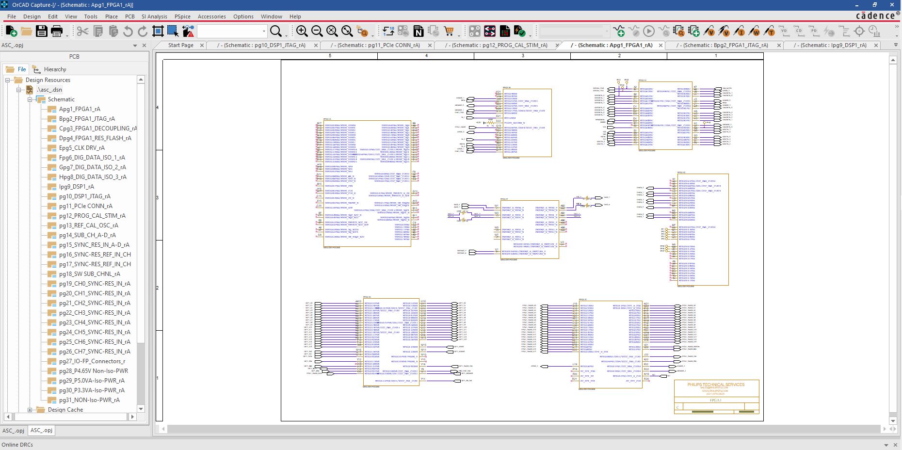
Extensive PCB Design experience with multi-layer boards with ASICs, BGA/FPGA packages with highly constrained high-speed buses. We have familiarity with all phases of hardware development including: Orcad Schematic Capture entry, signal integrity practices, constraint entry, library creation, DFM, Experience with a broad range of PCB form factors, also experienced with HDI / Blind and Buried Vias Type4 PCB design,
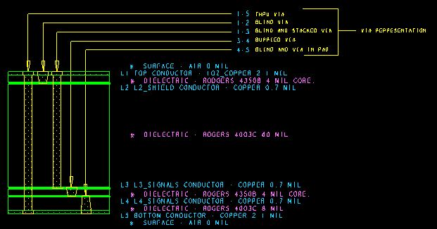
- VIA TYPES:
- TENTED VIAS: These are Type I vias where a mask material
bridges over it and no additional is present inside the hole. - TENTED AND COVERED VIAS: These are Type II vias with a
secondary covering of mask material covering the tented via. - PLUGGED VIAS: These are Type III vias with a material
partially penetrating the hole. - PLUGGED AND COVERED VIAS: These are Type IV vias with a
secondary covering of material over the type III vias. - FILLED VIAS: These are Type V vias with a material fully
penetrating and encapsulating the hole. - FILLED AND COVERED VIAS: These are Type VI vias with a
material covering the Type V vias. - FILLED AND CAPPED VIAS: These are Type VII vias with a metalized secondary coating covering the Type V vias.
Placement and routing studies to optimize new FPGA package ball maps , Experience with Impedance Control and Transmission Line applications, Excellent problem solving skills, Ownership of the layout from feasibility studies to board tape-out, Constraint entry of signal integrity guidelines, Interface with Manufacturing Engineers, Experience in PC, Tablet and motherboard designs, Experience with Analog design layout techniques, Along with Experience with RF design layout techniques as well,.
WHY P.T.S.
How A Private PCB Design Contractor Can Help You with a Project that You Were Told It Couldn’t be Done. When working with large corporations we work well with your engineering staff. With today’s state of the art technologies such as video conferencing, Microsoft Power Point and email for correspondence we can successfully communicate without the need of physically being there. This saves time and time is money. Maybe you are an entrepreneur like myself. I can help you get the job done as well by using other entrepreneurs with their own expertise this will help us with your job task. Whether it be more engineering services, or manufacturing and Assembly Services we will get you to the finish line cost effectively. We have experience with custom interposer designs for your flip chip technology or wire bonding needs to go to PCB. We use domestic and international services for our manufacturing services. Nevertheless, there are times when you will have a design that will need a designer that can do a design that is not the average PCB Design! That is where Philips Technical Service can help you. We understand the process of fabrication and if the components FIT, we can connect them with the minimum amount of signal layers to meet the constraints of your design. We specialize in PCB Design which is always done in house. We are a TurnKey design bureau by brokering engineering and mechanical design through local companies and we are also helping to support the local community and keeping costs down through competition. This also lets us use multiple references and resources to complete your design. I can go on and tell you how long I been doing this, Let’s just say I seen a lot advancements in the industry. By working with talented companies, we have great success going from silicon to organic PCB interposers with up 1200 connections in less than a sq. in. of area. So, depending on the complexity of your design it may pay for you to outsource it.
For ALL PHASES OF Printed Circuit Board Design Contact:
Philip Popalardo 631-979-0820
email:sales@philipsts.com email:info@philipsts.com Web:philipsts.com
PO BOX 63 RONKOKOMA, NY 11779